Difference between revisions of "Nano 3G"
LemonJesus (talk | contribs) (porting over my hardware notes) |
|||
| (8 intermediate revisions by 4 users not shown) | |||
| Line 2: | Line 2: | ||
[[Image:nano_3g_bck_a.png|500px]] | [[Image:nano_3g_bck_a.png|500px]] | ||
==Components== | ==Components== | ||
| − | {| | + | {| class="wikitable" |
| − | ! | + | ! Label !! Component !! Part !! Markings !! Notes |
|- | |- | ||
| + | | 2 | ||
| CPU | | CPU | ||
| − | |||
| Samsung S5L8702 | | Samsung S5L8702 | ||
| − | |337S3473 8702 | + | | 337S3473 8702, NONBWOEC, 0731 ARM |
| − | NONBWOEC | ||
| − | 0731 ARM | ||
| ARM926EJ-S processor. The package itself is Apple-branded and marked 337S3473 8702. | | ARM926EJ-S processor. The package itself is Apple-branded and marked 337S3473 8702. | ||
|- | |- | ||
| + | | 3 | ||
| SDRAM | | SDRAM | ||
| − | |||
| [http://www.samsung.com/global/system/business/semiconductor/product/2007/11/13/236652ds_k4x56163pi.pdf K4X56163PI] or Qimonda HYE18M169CX75 | | [http://www.samsung.com/global/system/business/semiconductor/product/2007/11/13/236652ds_k4x56163pi.pdf K4X56163PI] or Qimonda HYE18M169CX75 | ||
| − | |0728 | + | | 0728, C, HYE18M256, 169CX75, W3338092 |
| − | C | + | | SDRAM - Mobile DDR, 256Mb, 1.8V. WORK ON THIS: Like the flash chip, the memory also varies. The most popular chip seems to be the [http://www.samsung.com/global/system/business/semiconductor/product/2007/11/13/236652ds_k4x56163pi.pdf K4X56163PI]. Another similar one that is sometimes used is the Qimonda HYE18M169CX75 |
| − | HYE18M256 | ||
| − | 169CX75 | ||
| − | W3338092 | ||
| − | | WORK ON THIS: Like the flash chip, the memory also varies. The most popular chip seems to be the [http://www.samsung.com/global/system/business/semiconductor/product/2007/11/13/236652ds_k4x56163pi.pdf K4X56163PI]. Another similar one that is sometimes used is the Qimonda HYE18M169CX75 | ||
|- | |- | ||
| + | | 5 | ||
| Utility Flash | | Utility Flash | ||
| − | |||
| [http://www.sst.com/products/?inode=41340 SST25VF080B] | | [http://www.sst.com/products/?inode=41340 SST25VF080B] | ||
| − | | | + | | V80B, 729379 |
| − | | | + | | Flash - NOR, 8Mb, Serial SPI |
|- | |- | ||
| + | | 6 | ||
| NAND Flash | | NAND Flash | ||
| − | |||
| Varies | | Varies | ||
| − | |Samsung 728 | + | | Samsung 728, K9HCG08U5M, PCB0, FCF285X1 |
| − | K9HCG08U5M | ||
| − | PCB0 | ||
| − | FCF285X1 | ||
| | | | ||
|- | |- | ||
| + | | 1 | ||
| Audio codec | | Audio codec | ||
| − | |||
| WM1870 | | WM1870 | ||
| − | |APPLE | + | | APPLE, 338S0462, 76BZKTM |
| − | 338S0462 | ||
| − | 76BZKTM | ||
| | | | ||
|- | |- | ||
| + | | 4 | ||
| Power manager | | Power manager | ||
| − | |||
| D1671B | | D1671B | ||
| − | | | + | | 338S0408, 07258HAH |
| | | | ||
|} | |} | ||
| + | |||
| + | == SPI NOR Test Pads == | ||
| + | |||
| + | Test pads are available on the back of the board to access SCK, MISO and CS between the SoC and the NOR utility flash. MOSI is also present, but is buried in an internal layer (second from back) which can be accessed by carefully scraping off the top FR4 using a sharp tool, or by using a tiny carbide bit on a milling machine. | ||
| + | |||
| + | [[Image:N3g-spi-nor.png|500px]] | ||
| + | [[Image:N3g-spi-nor-zoom.png|500px]] | ||
| + | |||
| + | == Hardware Notes == | ||
| + | === CPU === | ||
| + | The Apple S5L8702 is an ARM926EJ-S processor designed by Samsung. It is estimated to run at 100MHz (I read this somewhere but I don't remember where). The basics of the chip are similar to the S5L8700x for which there is [[S5L8700 datasheet|a leaked datasheet]]. For some peripherals, merely a base address has changed. For others, full subsystems have been updated and refined. | ||
| + | |||
| + | === GPU === | ||
| + | Very little is known about the GPU core other than the fact that it almost certainly exists. It's likely a single PowerVR GPU core that can maybe can decode H.264 content up to 480p (or perhaps there's another peripheral responsible for this?). It's also possible that the GPU is responsible for rendering games, since it appears the games use some form of OpenGL ES. CoverFlow also probably leverages the GPU. | ||
| + | |||
| + | === I2C === | ||
| + | The S5L8702 has several I2C busses (two, probably?), but possibly only one is used (bus #0). On this bus, there are currently two known slaves: | ||
| + | * The PMU at address 0x73 | ||
| + | * The DAC at address 0x1A | ||
| + | The bus runs at 1.8V with a clock of 333.33KHz. | ||
| + | |||
| + | Other notes about the I2C peripheral from Rockbox: | ||
| + | * s5l8702 I2C controller is similar to s5l8700, known differences are: | ||
| + | ** IICCON[5] is not used in s5l8702. | ||
| + | ** IICCON[13:8] are used to enable interrupts. | ||
| + | ** IICSTA2[13:8] are used to read the status and write-clear interrupts. | ||
| + | * Known interrupts: | ||
| + | ** [13] STOP on bus (TBC) | ||
| + | ** [12] START on bus (TBC) | ||
| + | ** [8] byte transmitted or received in Master mode (not tested in Slave) | ||
| + | ** IICCON[4] does not clear interrupts, it is enabled when a byte is transmited or received, in Master mode the tx/rx of the next byte starts when it is written as "1". | ||
| + | |||
| + | === Digital Audio Subsystem (I2S) === | ||
| + | The iPod n3g uses a Wolfson DAC (WM1870) to convert digital audio to analog audio. The S5L8702 sends digital audio in the form of I2S data at 44.1kHz with 16-bit resolution. Even if there is no audio playing, at some point during boot up, the I2S peripheral is turned on, meaning the Bit Clock and Word Select are always on. During the 1kHz tone test in the diagnostic menu, the I2S mode is different, possibly a half-data mode since the test tone is one channel. | ||
| + | The S5L8702 seems to support 3 I2S interfaces, but only one is used for audio playback. It's possible another one is used for microphone recording (when an Apple headset with a microphone is plugged in, you can record voice memos) but this is unconfirmed. | ||
| + | |||
| + | The S5L8702 sends data to the DAC at full volume no matter what. Volume is configured via I2C bus #0. As far as I can tell, two commands are issued to change the volume: | ||
| + | Address 0x1A, Data 0x04 <volume> | ||
| + | Address 0x1A, Data 0x07 <volume> | ||
| + | Where <volume> is a number between 0xB7 for quietest to 0xF5 for loudest. It's also possible that a special value of 0x80 is for full mute, but this is unconfirmed. It's also unclear what the 0x04 and 0x07 mean, perhaps it's capable of changing the volume of both channels independently? | ||
| + | |||
| + | Both the I2C and I2S busses run at 1.8V. | ||
| + | |||
| + | === NAND === | ||
| + | NAND hardware is an enigma. There has been a rather substantial effort on this subsystem alone. Most of that is documented [https://github.com/lemonjesus/S5L8702-FMISS-Tools here]. | ||
| + | |||
==Helpful pages== | ==Helpful pages== | ||
Chip analyses: | Chip analyses: | ||
Latest revision as of 22:19, 19 November 2023
Contents
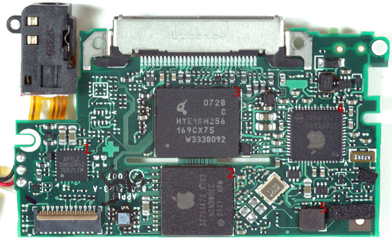
Components
| Label | Component | Part | Markings | Notes |
|---|---|---|---|---|
| 2 | CPU | Samsung S5L8702 | 337S3473 8702, NONBWOEC, 0731 ARM | ARM926EJ-S processor. The package itself is Apple-branded and marked 337S3473 8702. |
| 3 | SDRAM | K4X56163PI or Qimonda HYE18M169CX75 | 0728, C, HYE18M256, 169CX75, W3338092 | SDRAM - Mobile DDR, 256Mb, 1.8V. WORK ON THIS: Like the flash chip, the memory also varies. The most popular chip seems to be the K4X56163PI. Another similar one that is sometimes used is the Qimonda HYE18M169CX75 |
| 5 | Utility Flash | SST25VF080B | V80B, 729379 | Flash - NOR, 8Mb, Serial SPI |
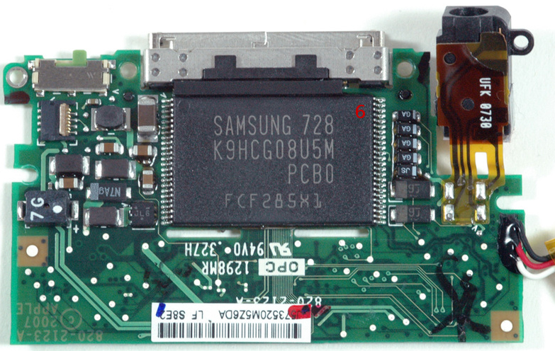
| 6 | NAND Flash | Varies | Samsung 728, K9HCG08U5M, PCB0, FCF285X1 | |
| 1 | Audio codec | WM1870 | APPLE, 338S0462, 76BZKTM | |
| 4 | Power manager | D1671B | 338S0408, 07258HAH |
SPI NOR Test Pads
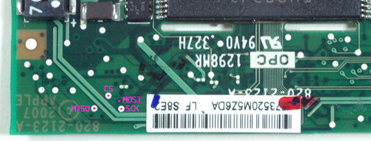
Test pads are available on the back of the board to access SCK, MISO and CS between the SoC and the NOR utility flash. MOSI is also present, but is buried in an internal layer (second from back) which can be accessed by carefully scraping off the top FR4 using a sharp tool, or by using a tiny carbide bit on a milling machine.
Hardware Notes
CPU
The Apple S5L8702 is an ARM926EJ-S processor designed by Samsung. It is estimated to run at 100MHz (I read this somewhere but I don't remember where). The basics of the chip are similar to the S5L8700x for which there is a leaked datasheet. For some peripherals, merely a base address has changed. For others, full subsystems have been updated and refined.
GPU
Very little is known about the GPU core other than the fact that it almost certainly exists. It's likely a single PowerVR GPU core that can maybe can decode H.264 content up to 480p (or perhaps there's another peripheral responsible for this?). It's also possible that the GPU is responsible for rendering games, since it appears the games use some form of OpenGL ES. CoverFlow also probably leverages the GPU.
I2C
The S5L8702 has several I2C busses (two, probably?), but possibly only one is used (bus #0). On this bus, there are currently two known slaves:
- The PMU at address 0x73
- The DAC at address 0x1A
The bus runs at 1.8V with a clock of 333.33KHz.
Other notes about the I2C peripheral from Rockbox:
- s5l8702 I2C controller is similar to s5l8700, known differences are:
- IICCON[5] is not used in s5l8702.
- IICCON[13:8] are used to enable interrupts.
- IICSTA2[13:8] are used to read the status and write-clear interrupts.
- Known interrupts:
- [13] STOP on bus (TBC)
- [12] START on bus (TBC)
- [8] byte transmitted or received in Master mode (not tested in Slave)
- IICCON[4] does not clear interrupts, it is enabled when a byte is transmited or received, in Master mode the tx/rx of the next byte starts when it is written as "1".
Digital Audio Subsystem (I2S)
The iPod n3g uses a Wolfson DAC (WM1870) to convert digital audio to analog audio. The S5L8702 sends digital audio in the form of I2S data at 44.1kHz with 16-bit resolution. Even if there is no audio playing, at some point during boot up, the I2S peripheral is turned on, meaning the Bit Clock and Word Select are always on. During the 1kHz tone test in the diagnostic menu, the I2S mode is different, possibly a half-data mode since the test tone is one channel. The S5L8702 seems to support 3 I2S interfaces, but only one is used for audio playback. It's possible another one is used for microphone recording (when an Apple headset with a microphone is plugged in, you can record voice memos) but this is unconfirmed.
The S5L8702 sends data to the DAC at full volume no matter what. Volume is configured via I2C bus #0. As far as I can tell, two commands are issued to change the volume:
Address 0x1A, Data 0x04 <volume>
Address 0x1A, Data 0x07 <volume>
Where <volume> is a number between 0xB7 for quietest to 0xF5 for loudest. It's also possible that a special value of 0x80 is for full mute, but this is unconfirmed. It's also unclear what the 0x04 and 0x07 mean, perhaps it's capable of changing the volume of both channels independently?
Both the I2C and I2S busses run at 1.8V.
NAND
NAND hardware is an enigma. There has been a rather substantial effort on this subsystem alone. Most of that is documented here.
Helpful pages
Chip analyses:
Teardowns:


