Nano 5G
Nano 5G
Components
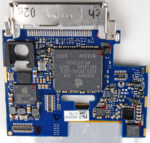
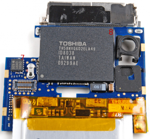
| Label | Component | Part | Markings | Notes |
|---|---|---|---|---|
| 2 | CPU | Samsung S5L8730 | 339S0081 ARM, K4X51323PG-UGC6, EDE168AG 0928, APL0378A00, N1X2XW 0931 | Printed backwards on the chip - how sneaky. ARM1176JZF-S core (per CP15 data). |
| SDRAM | Integrated into the processor, similar to the iPod Touch and iPhone lines. | |||
| 8 | NAND Flash | Various 8/16 GB chips | TH58NVG6D2ELA49, ID8038, TAIWAN, 09299AE | One example is TH58NVG6D2ELA49 visible on the iFixit Teardown |
| 1 | Power manager | Probably Dialog | 338S0707, -AD, 09278HGZ | Similar looking and named chips like this have been power managers. Apple uses chips like these in just about every device. |
| 3 | ||||
| 4 | ||||
| 5 | Audio codec | Cirrus Logic CLI1480A | 338S0559, ATWV0926, SGP | Also found in the Touch 3G. Stereo CODEC w/ Headphone and Speaker Amp |
| 6 | Accelerometer | LIS331DLM | 33DM, 2910 | The newer Touch's, iPhone's, and even the iPad have similar accelerometers, and I've discovered a pattern in the chip names. |
| 7 | 0630, CK9Y, 925 |
CP15 Registers
Dump of CP15 registers from bootrom context:
| cX | cY | opc2 | Description | Value | Interpretation |
|---|---|---|---|---|---|
| 0 | 0 | 0 | Main ID | 410fb764 | ARM (0x41), Variant 0, Architecture: see CPUID, Part: ARM1176 |
| 0 | 0 | 1 | Cache Type | 1d152152 | Write back, format C cache lockdown, Register 7 cache cleaning operations, separate I/D caches; data cache: (no restriction on page allocation, 16KB, 4-way associative, 2 word line length) istrunction cache: (no restrictions on page allocation, 16KB, 4-way, 2 word) |
| 0 | 0 | 2 | TCM Status | 00000000 | No tightly coupled memory. |
| 0 | 0 | 3 | TLB Type | 00000800 | |
| 0 | 1 | 0 | Processor Feature 0 | 00000111 | Jazelle, Thumb1, ARM (no Thumb2) |
| 0 | 1 | 1 | Processor Feature 1 | 00000011 | Security Extensions Architecture v1, Standard ARMv4 programmer's model. No microcontroller model. |
| 0 | 1 | 2 | Debug Feature 0 | 00000033 | v6.1 Secure Debug, v6.1 Debug. |
| 0 | 1 | 3 | Auxiliary Feature 0 | 00000000 | |
| 0 | 1 | 4 | Memory Model Feature 0 | 01130003 | Standard ARM1176JZF-S. |
| 0 | 1 | 5 | Memory Model Feature 1 | 10030302 | Standard ARM1176JZF-S. |
| 0 | 1 | 6 | Memory Model Feature 2 | 01222100 | Standard ARM1176JZF-S. |
| 0 | 1 | 7 | Memory Model Feature 3 | 00000000 | Standard ARM1176JZF-S. |
| 0 | 2 | 0 | Instruction Set Feature Attribute 0 | 00140011 | Standard ARM1176JZF-S. |
| 0 | 2 | 1 | Instruction Set Feature Attribute 1 | 12002111 | Standard ARM1176JZF-S. |
| 0 | 2 | 2 | Instruction Set Feature Attribute 2 | 11231121 | Standard ARM1176JZF-S. |
| 0 | 2 | 3 | Instruction Set Feature Attribute 3 | 01102131 | Standard ARM1176JZF-S. |
| 0 | 2 | 4 | Instruction Set Feature Attribute 4 | 00001141 | Standard ARM1176JZF-S. |
| 0 | 2 | 5 | Instruction Set Feature Attribute 5 | 00000000 | Standard ARM1176JZF-S. |
| 1 | 0 | 0 | Control | 00450078 | No Force AP, no TEX remap, CPSR E set to 0 on exception, no VIC, no extended page tables, allow unaligned data access, no fast interrupts, global enable for instruction/data TCM, loads to PC set the T bit, random cache replacement, exceptions vectors at Vector Base Address Register. I$, D$ disabled by wInd3x, branch prediction disabled, no strict alignment fault checking, no MMU. |
| 1 | 0 | 1 | Auxiliary Control | 00000007 | ... |
| 1 | 0 | 2 | Coprocessor Access Control | 00000000 | ... |
| 1 | 1 | 0 | Secure Configuration | 00000000 | ... |
| 1 | 1 | 1 | Secure Debug Enable | 00000000 | ... |
| 1 | 1 | 2 | Non-Secure Access Control | 00000000 | ... |
| 2 | 0 | 0 | Translation Table Base 0 | 00000000 | ... |
| 2 | 0 | 1 | Translation Table Base 1 | 00000000 | ... |
| 2 | 0 | 2 | Translation Table Base Control | 00000000 | ... |
| 3 | 0 | 0 | Domain Access Control | 00000000 | ... |
| 7 | 4 | 0 | PCA | 00000000 | ... |
| 7 | 10 | 6 | Cache Dirty Status | 00000000 | ... |
| 9 | 0 | 0 | Data Cache Lockdown | fffffff0 | ... |
| 9 | 0 | 1 | Instruction Cache Lockdown | fffffff0 | ... |
| 9 | 1 | 0 | Data TCM Region | 00000000 | ... |
| 9 | 1 | 1 | Instruction TCM Region | 00000000 | ... |
| 9 | 1 | 2 | Data TCM Non-secure Control Access | 00000000 | ... |
| 9 | 1 | 3 | Instruction TCM Non-secure Control Access | 00000000 | ... |
| 9 | 2 | 0 | TCM Selection | 00000000 | ... |
| 9 | 8 | 0 | Cache Behavior Override | 00000000 | ... |
Clock Gates
The clock gate registers are:
| Address | Name |
|---|---|
| 0x3C500048 | GATES[0] |
| 0x3C50004C | GATES[1] |
| 0x3C500058 | GATES[4] |
| 0x3C500068 | GATES[8] |
| 0x3C50006C | GATES[9] |
GATES[2, 3, 5, 6, 7], etc seem to be unused. A clock is enabled by setting a corresponding bit (GATE[n][m]) low. The following clock gates have been extracted by analyzing debug structures in OSOS. We also provide the 'numerical' argument that can be passed to the clkgen_{enable,disable}_gate function calls in the BootROM. The BootROM will automatically enable some function-related gates together if one is specified. This is probably a leftover from earlier codebases where one functionality would correspond to one clock gate bit, while now a functionality might be gated behind multiple bits.
| Function | Register(s)/Bit(s) | Number in BootROM |
|---|---|---|
| AES | GATE[0][7] | 7 |
| AMC | GATE[0][3] | 3 |
| AMC-core | GATE[0][4] | 4 |
| AMCSS | GATE[1][17] | 38 |
| ARM-core | GATE[0][15] | 15 |
| ARM-icu | GATE[0][16] | 16 |
| ARM-sleep | GATE[0][20] | 20 |
| AXI-bus | GATE[1][18] | 39 |
| AXI-spine | GATE[8][13] | 63 |
| AXI-video | GATE[8][14] | 64 |
| CAMIF | GATE[0][17], GATE[8][15] | 17, 65 |
| CEATA | GATE[0][6] | 6 |
| CLCD | GATE[8][9] | 59 |
| CLCD-OTF | GATE[8][10] | 60 |
| CSIS | GATE[0][18] | 18 |
| DDR-MIU | GATE[9][17] | 89 |
| DMAC0 | GATE[0][11] | 11 |
| DMAC1 | GATE[0][12] | 12 |
| DMAX | GATE[8][8] | 58 |
| ECC | GATE[0][9] | 9 |
| ECID | GATE[1][14] | 35 |
| FMC | GATE[0][5] | 5 |
| GPIO | GATE[1][12] | 33 |
| H264 | GATE[8][2], GATE[9][18] | 52, 90 |
| H264ENC | GATE[4][7], GATE[8][16], GATE[8][17] | 60, 66, 67 |
| IIC0 | GATE[1][4], GATE[9][11] | 25, 83 |
| IIC1 | GATE[1][6], GATE[9][12] | 27, 84 |
| IIS0 | GATE[1][7] | 28 |
| IIS1 | GATE[1][10] | 31 |
| IIS2 | GATE[1][16] | 37 |
| JPEG | GATE[0][19] | 19 |
| LCD | GATE[0][1], GATE[9][16] | 1, 88 |
| MBX-3D | GATE[8][6] | 56 |
| MBX-bus | GATE[8][7] | 57 |
| MBX-core | GATE[8][5] | 55 |
| MIPI-link | GATE[1][19] | 40 |
| MIXER | GATE[8][1] | 51 |
| MPVD | GATE[8][3] | 53 |
| PKE | GATE[1][13] | 34 |
| PL301MPVD | GATE[1][21] | 42 |
| PRNG | GATE[1][0] | 21 |
| RINGOSC | GATE[4][0] | 53 |
| SCALER | GATE[8][4], GATE[9][25] | 54, 97 |
| SDIO | GATE[0][8] | 8 |
| SHA1 | GATE[0][0] | 0 |
| SPD | GATE[1][8] | 29 |
| SPI0 | GATE[1][2], GATE[9][13] | 23, 85 |
| SPI1 | GATE[1][11], GATE[9][14] | 32, 86 |
| SPI2 | GATE[1][15], GATE[9][15] | 36, 87 |
| SPI3 | GATE[4][1], GATE[9][19] | 54, 91 |
| SPI4 | GATE[4][4], GATE[9][20] | 57, 92 |
| SWI | GATE[4][2], GATE[9][21] | 55, 93 |
| TIMER0 | GATE[1][5], GATE[9][0] | 26, 72 |
| TIMER1 | GATE[1][23], GATE[9][1] | 44, 73 |
| TIMER2 | GATE[1][24], GATE[9][2] | 45, 74 |
| TIMER3 | GATE[1][25], GATE[9][3] | 46, 75 |
| TIMER4 | GATE[1][26], GATE[9][4] | 47, 76 |
| TIMER5 | GATE[1][27], GATE[9][5] | 48, 77 |
| TIMER6 | GATE[1][28], GATE[9][6] | 49, 78 |
| TIMER7 | GATE[4][5], GATE[9][22] | 58, 94 |
| TIMER8 | GATE[4][6], GATE[9][23] | 59, 95 |
| TVOUT | GATE[0][10] | 10 |
| TW | GATE[1][1] | 22 |
| UART0 | GATE[1][9], GATE[9][7] | 30, 79 |
| UART1 | GATE[1][29], GATE[9][8] | 50, 80 |
| UART2 | GATE[1][30], GATE[9][9] | 51, 81 |
| UART3 | GATE[1][31], GATE[9][10] | 52, 82 |
| UART4 | GATE[4][8], GATE[9][26] | 61, 98 |
| USB-OTG | GATE[0][2] | 2 |
| USB2-PHY | GATE[1][3] | 24 |
| VP | GATE[8][0] | 50 |
| VROM | GATE[0][13] | 13 |
| XMC | GATE[8][12] | 62 |
Helpful pages
Teardowns:
Other:

