S5L8701 analysis
Introduction
The samsung S5L8701 is the SOC of the IN2G. This chip is supposed to be close to the 8700 used on some concurrent MP3 players.
We currently know nearly nothing about the differences of both chips, and the further evolutions. There is probably a small unencrypted boot ROM inside, which would be very usefull for integrating user SW. Probably containing crypto information. Knowing the location of some JTAG pins could be very helpfull.
Structure of the packaging
The chip is a 226-pin TFBGA with a pitch of 0.5mm. This is the structure of a BGA package : BGA package
The chip is glued to a small double side PCB substrat. the electrical current passes through :
-a pad of the chip die
-a bonding wire
-the top layer of the substrate
-a via
-the bottom layer
-finally, the BGA ball
The [[known datasheet]S5L8700_datasheet] shows die pad numbers that need to be correlated to ball numbers (the specified package has a different ball layout). In order to do this, we make an analysis of the bonding and PCB.
Packaging analysis
Following steps were made :
-desoldering of the IC
-removing of the balls and filler glue
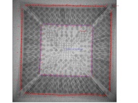
-X-ray picture
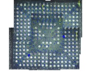
-microscope picture ot the bottom layer
-removing the bottom layer and most of the substrate (by careful manual grinding)
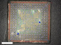
-microscope picture of the top layer
-superposition of these views, and path finding from the die to the ball


