Nano 4G: Difference between revisions
No edit summary |
User890104 (talk | contribs) No edit summary |
||
| (7 intermediate revisions by 3 users not shown) | |||
| Line 1: | Line 1: | ||
{{DISPLAYTITLE:iPod nano (4th generation)}} | |||
==Components== | ==Components== | ||
[[File:nano_4g_frt_a.png|500px|thumb|none|Front of the circuit board]] | |||
[[File:nano_4g_bck_a.png|500px|thumb|none|Back of the circuit board]] | |||
{| class="wikitable" | {| class="wikitable" | ||
! Label !! Component !! Part !! Markings !! Notes | ! Label !! Component !! Part !! Markings !! Notes | ||
| Line 9: | Line 10: | ||
| Samsung S5L8720 | | Samsung S5L8720 | ||
| 339S0049 ARM, K4X56323PI-KGC4, YWE025QH 825, APL0278A00, N1B2HOP 0831 | | 339S0049 ARM, K4X56323PI-KGC4, YWE025QH 825, APL0278A00, N1B2HOP 0831 | ||
| ARM1176JZF-S processor. It is definitely worth knowing that this is the exact same processor used in the iTouch 2G. This could mean that some of the same exploits for that could possibly be used. [ | | ARM1176JZF-S processor. It is definitely worth knowing that this is the exact same processor used in the iTouch 2G. This could mean that some of the same exploits for that could possibly be used. [https://theapplewiki.com/wiki/S5L8720/Hardware S5L8720/Hardware] is a very interesting page on the Apple wiki. | ||
|- | |- | ||
| | | | ||
| Line 19: | Line 20: | ||
| 4 | | 4 | ||
| Accelerometer | | Accelerometer | ||
| [http://www.st.com/stonline/products/ | | [http://www.st.com/stonline/products/literature/ds/12726.pdf LIS302DL] | ||
| 33DL, 2827 | | 33DL, 2827 | ||
| The newer Touch's, iPhone's, and even the iPad have similar accelerometers, and I've discovered a pattern in the chip names. | | The newer Touch's, iPhone's, and even the iPad have similar accelerometers, and I've discovered a pattern in the chip names. | ||
| Line 37: | Line 38: | ||
| 1 | | 1 | ||
| Power manager | | Power manager | ||
| D1759 | | Dialog D1759 | ||
| 338S0687-AC, 08288HBB | | 338S0687-AC, 08288HBB | ||
| | | | ||
| Line 46: | Line 47: | ||
| | | | ||
| | | | ||
|} | |||
== Bootrom == | |||
See [[S5L8720 Bootrom]]. Different from the S5L8720 bootrom used in the iPod Touch 2G (which is iBoot-based, a.k.a. SecureROM). | |||
== Memory Map == | |||
See [https://www.theiphonewiki.com/wiki/S5L8720_(Hardware)] and [https://code.google.com/archive/p/chronicdev/wikis/N72APDevTree.wiki]. | |||
In addition to the above, a few extra memory regions have been found while reverse engineering the [[S5L8720 Bootrom]]: | |||
{| class="wikitable" | |||
! Name !! Address !! Notes | |||
|- | |||
| Mystery DMA | |||
| 0x3880_0000 | |||
| A PL080-like DMA engine, but with slightly different MMIO register structure. Used by the [[S5L8720 Bootrom|bootrom]] to copy the DFU payload from 0x2200_0600 to 0x2200_0000 after decryption and verification. Or maybe that's actually doing the decryption? To be investigated. | |||
|- | |||
| Mystery Interrupt Thing | |||
| 0x39a0_0000 | |||
| Not the VICs (0x38e0_0000, 0x38e0_1000), not the EdgeIC (0x38e0_2000). Seems to hold 7 different 32-bit registers for interrupt status at 0xa0, and 7 different 32-bit registers for interrupt mask at 0xc0. The 7 different registers correspond to 7 'modes' of ISRs set up in the bootrom. Not much is known about what it does, and what these 'modes' are. To be investigated. | |||
|} | |} | ||
Latest revision as of 19:16, 6 January 2026
Components


| Label | Component | Part | Markings | Notes |
|---|---|---|---|---|
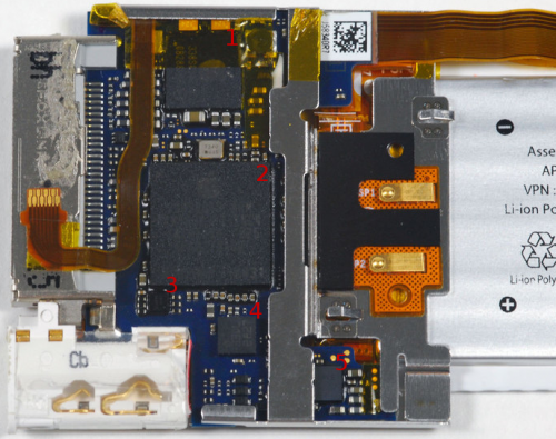
| 2 | CPU | Samsung S5L8720 | 339S0049 ARM, K4X56323PI-KGC4, YWE025QH 825, APL0278A00, N1B2HOP 0831 | ARM1176JZF-S processor. It is definitely worth knowing that this is the exact same processor used in the iTouch 2G. This could mean that some of the same exploits for that could possibly be used. S5L8720/Hardware is a very interesting page on the Apple wiki. |
| SDRAM | 32MB, probably MDDR. Integrated into the processor, similar to the iPod Touch and iPhone lines. | |||
| 4 | Accelerometer | LIS302DL | 33DL, 2827 | The newer Touch's, iPhone's, and even the iPad have similar accelerometers, and I've discovered a pattern in the chip names. |
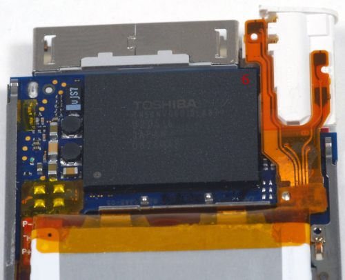
| 6 | NAND Flash | Varies | TH58NVG6D1DLA87, U20516, JAPAN, 0826MAE | |
| 5 | Audio codec | CS42L58 | 338S055C, 189N0824, SGP | I determined this because the iPod nano (5th generation) has a similar chip, which we are sure of the identity. One person lifted this chip and found that the pins connect to the LCD connector. Not much info was given, and it could just be a common ground, but the identity of this chip is still up in the air. |
| 1 | Power manager | Dialog D1759 | 338S0687-AC, 08288HBB | |
| 3 |
Bootrom
See BootROM. Different from the S5L8720 bootrom used in the iPod Touch 2G (which is iBoot-based, a.k.a. SecureROM).
Memory Map
In addition to the above, a few extra memory regions have been found while reverse engineering the BootROM:
| Name | Address | Notes |
|---|---|---|
| Mystery DMA | 0x3880_0000 | A PL080-like DMA engine, but with slightly different MMIO register structure. Used by the bootrom to copy the DFU payload from 0x2200_0600 to 0x2200_0000 after decryption and verification. Or maybe that's actually doing the decryption? To be investigated. |
| Mystery Interrupt Thing | 0x39a0_0000 | Not the VICs (0x38e0_0000, 0x38e0_1000), not the EdgeIC (0x38e0_2000). Seems to hold 7 different 32-bit registers for interrupt status at 0xa0, and 7 different 32-bit registers for interrupt mask at 0xc0. The 7 different registers correspond to 7 'modes' of ISRs set up in the bootrom. Not much is known about what it does, and what these 'modes' are. To be investigated. |
Reverse Engineering Results
Timers: These clockgates have been found to be related to timers: 37, 55, 56, 57, 58, 59, 60, 69, 70, 128, 129, 130, 131, 132, 133, 134, 150 and 151.
Status registers
We dumped all c0 coprocessor registers:
c0,c0
Value: 0x410FB764
Interpretation: ARM1176 rev. 4
c0,c1
Value: 0x1D152152
Interpretation: DCache/ICache 16KB each, 4 way associative, 32 bytes line size
c0,c2
Value: 0x00000000
Interpretation: No TCM
c0,c3
Value: 0x00000800
Interpretation: Unified TLB, 8 lockable entries
c1,c0
Value: 0x00000111
Interpretation: ARM/Thumb1/Jazelle support, no Thumb2 support
c1,c1
Value: 0x00000011
Interpretation: Trustzone v1
c1,c2
Value: 0x00000033
Interpretation: Supports debug model v6.1, both applications processor and secure
c1,c3
Value: 0x00000000
Interpretation: No auxiliary features
c1,c4
Value: 0x01130003
Interpretation: FCSE, Auxiliary Control register, ARMv6 TCM/DMA, no DMA cache coherency, no multicore cache coherency, VMSA v7
c1,c5
Value: 0x10030302
Interpretation: Branch target buffer, Harvard architecture, various cache operations supported (see TRM)
c1,c6
Value: 0x01222100
Interpretation: WFI, Data synchronization barrier, Prefetch flush, Data memory barrier, various TLB/cache operations supported (see TRM), no prefetch cache range operation
c1,c7
Value: 0x00000000
Interpretation: No hierarchical cache maintenance support
c2,c0
Value: 0x00140011
Interpretation: Supports BKPT, CDP, CDP2, LDC, LDC2, MCD, MCD2, MRC, MRC2, STC, STC2, MCRR, MCRR2, MRRC, MRRC2, CLZ, SWP and SWPB, doesn't support division, combined compare and branch or bitfield instructions
c2,c1
Value: 0x12002111
Interpretation: Supports BXJ, BX, BLX, PC loads have BX behavior, supports SXTB, SXTAB, SXTB16, SXTAB16, SXTH, SXTAH, UXTB, UXTAB, UXTB16, UXTAB16, UXTH, UXTAH, SRS, RFE, CPS, LDM(2), LDM(3), STM(2) and SETEND
c2,c2
Value: 0x11231121
Interpretation: Supports REV, REV16, REVSH, MRS, MSR, UMULL, UMLAL, UMAAL, SMULL, SMLAL, SMLABB, SMLABT, SMLALBB, SMLALBT, SMLALTB, SMLALTT, SMLATB, SMLATT, SMLAWB, SMLAWT, SMULBB, SMULBT, SMULTB, SMULTT, SMULWB, SMULWT, SMLAD, SMLADX, SMLALD, SMLALDX, SMLSD, SMLSDX, SMLSLD, SMLSLDX, SMMLA, SMMLAR, SMMLS, SMMLSR, SMMUL, SMMULR, SMUAD, SMUADX, SMUSD, SMUSDX, MLA, restartable LDM/STM, PLD, LDRD, STRD and Q bit in PSRs
c2,c3
Value: 0x01102131
Interpretation: Supports true NOP, Thumb MOV(3)/CPU, LDREX, STREX, LDREXB, LDREXH, LDREXD, STREXB, STREXH, STREXD, CLREX, SVC, PKHBT, PKHTB, QADD16, QADD8, QADDSUBX, QSUB16, QSUB8, QSUBADDX, SADD16, SADD8, SADDSUBX, SEL, SHADD16, SHADD8, SHADDSUBX, SHSUB16, SHSUB8, SHSUBADDX, SSAT, SSAT16, SSUB16, SSUB8, SSUBADDX, SXTAB16, SXTB16, UADD16, UADD8, UADDSUBX, UHADD16, UHADD8, UHADDSUBX, UHSUB16, UHSUB8, UHSUBADDX, UQADD16, UQADD8, UQADDSUBX, UQSUB16, UQSUB8, UQSUBADDX, USAD8, USADA8, USAT, USAT16, USUB16, USUB8, USUBADDX, UXTAB16, UXTB16, QADD, QDADD, QDSUB, QSUB, and the Q and GE[3:0] bits in the PSRs. Does nut support branch table and Thumb2 instructions.
c2,c4
Value: 0x00001141
Interpretation: Supports SMC, writeback instructions, shift of loads and stores by 0-3 bits to the left, constant shift options, register controlled shift options, LDRBT, LDRT, STRBT and STRT. No barrier instructions support.
c2,c5
Value: 0x00000000
Interpretation: No additional implementation defined instruction set extensions
Helpful pages
Teardowns:
Other: